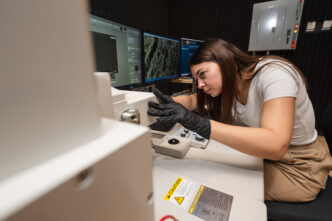
PENDLETON — Clemson University has expanded its microscopy capabilities available to private industry for the analysis of materials used in advanced manufacturing, health care, bio-engineering, aerospace and many other applications.
The university has installed state-of-the-art combined X-ray Photoelectron Spectroscopy (XPS) and Auger Electron Spectroscopy (AES) equipment at the multi-user Electron Microscopy Facility in the Advanced Materials Research Laboratory (AMRL) in Anderson County. Unique in the Southeast, the equipment allows scientists to analyze very thin surface layers of materials in ways not previously possible at Clemson.
This capability has been highly sought by Clemson researchers working on advanced materials, bio-materials, advanced manufacturing, health care, digital and information technology and environmental projects. The equipment will directly contribute to ongoing polymer, fiber and textile research; new catalyst developments; biological implants and biomedical research; geochemical research; alternative energy technology development; and all aspects of surface science-based projects at Clemson University and regional educational institutions, as well as private industry.
“The AMRL is just such a gem here that other businesses should look into,” said John Martin, new product development manager at Ulbrich Precision Flatwire, which produces extremely thin, highly engineered flat wire at its Westminster facility for use in medical devices, solar panels, batteries, satellites and numerous other products that require durability in extreme temperatures and conditions.
Many of Ulbrich’s products are thinner than a human hair and barely detectable to the human eye. The company uses Clemson advanced microscopy equipment to analyze its materials at the nanoscale to engineer its products and to provide information to clients using Ulbrich materials in its products.
“We get instant feedback,” Martin said.
Housing such high-powered, sensitive equipment internally can be too costly, Martin said, and Clemson scientists provide the technical expertise needed to maximize the benefit of the equipment.
The company employs Clemson University students as interns; some have stayed with Ulbrich after graduating.
“It’s just a win-win for everybody,” said Martin, a Clemson alumnus. “The students get great real-world experience and are functioning as professional engineers practically when they’re finished working with us.”
Ulbrich is just one of many industrial users at the facility.
KEMET Corp. of Simpsonville has been collaborating with Clemson’s Electron Microscopy Facility for more than 15 years to develop a better understanding of the various micro-structural effects of materials processing and chemistry. KEMET develops and manufactures capacitors used in electronics, ranging from handheld devices, medical implants, automotive and aerospace systems, and other electronics used around the world.
Javaid Qazi, KEMET senior manager of technical services, said the sophisticated material analysis capabilities from micro to nano range, along with the necessary technical expertise and confidentiality at Clemson’s facility, have been very helpful over the years.
“I am happy to see that what started purely as an electron microscopy lab has diversified over the years to add new analysis techniques,” Qazi said. “We can now do surface-depth profiling, for example, which is helpful in understanding the very thin coatings used on biomedical, automotive, aerospace and many other applications.”
The Electron Microscopy Facility features floor isolation and noise reduction to accommodate the highly sensitive equipment. Clemson faculty and private industry interested in using the facility can schedule time at the facility’s website at Clemson.edu/electronmicroscope, said Laxmikant Saraf, executive director of the facility.
“We greatly appreciate our industry collaborations because they help us maintain a world-class facility and also generate wonderful learning opportunities for our students,” Saraf said.
The facility was founded in the mid-1990s through a partnership with Hitachi High Technologies America Inc., which continues to support the Electron Microscopy Facility. The Electron Microscopy Facility, which houses some of the world’s most cutting-edge microscopes, has been hailed as a national model. Officials from Georgia Tech, Harvard University and others have visited campus to see it.
“Our long-term partnership with Clemson allows us to showcase our most advanced technology,” said Phil Bryson, Hitachi vice president and general manager. “The breadth and depth of advanced research and development being done at the facility is second to none. We’re proud to be a part of this fine institution.”
In addition to the new X-ray Photoelectron Spectroscopy and Auger Electron Spectroscopy equipment, the facility is equipped with variable-pressure and high-resolution scanning electron microscopes and transmission electron microscopes, as well as a gas sorption analyzer and a double-beam microscope. A complete list of the facility’s microscopes and capabilities is available online.
“This latest expansion represents a significant investment in one of Clemson’s core research facilities and provides our researchers and the private industry a unique platform for testing materials, while creating a wonderful opportunity for students to learn on the latest technologies available,” said Tanju Karanfil, Clemson University’s vice president for research.